Understanding Printed Circuit Boards (PCBs): Single, Double, and Multilayer Designs
Understanding Printed Circuit Boards (PCBs): Single, Double, and Multilayer Designs
A Printed Circuit Board (PCB) is the foundation of nearly every modern electronic device. From consumer electronics and industrial equipment to automotive systems and telecommunications products, PCBs provide the mechanical support and electrical connections required for electronic components to function efficiently and reliably.
As electronic products continue to become smaller, faster, and more complex, PCB technology has evolved from simple single-layer boards to highly sophisticated multilayer structures. Understanding the differences between these PCB types can help engineers, buyers, and manufacturers choose the right solution for their applications.
What Is a PCB?
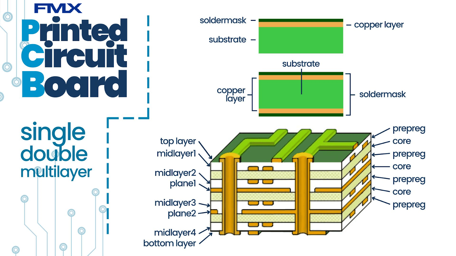
A PCB consists of conductive copper layers laminated onto an insulating substrate material. Electronic components are mounted onto the board and connected through copper traces that carry electrical signals and power throughout the circuit.
A standard PCB structure typically includes:
- Copper Layer – Conductive pathways for electrical signals
- Substrate/Core – Insulating base material, commonly FR4
- Solder Mask – Protective coating that prevents oxidation and short circuits
- Silkscreen – Printed markings for component identification and assembly guidance
Modern PCB manufacturing combines precision engineering, material science, and advanced fabrication technologies to meet increasingly demanding performance requirements.
Single-Sided PCB
A single-sided PCB contains one conductive copper layer on one side of the substrate. This is the simplest and most cost-effective PCB design.
Features
- Easy to design and manufacture
- Low production cost
- Suitable for simple circuits
- Ideal for high-volume consumer products
Common Applications
- LED lighting
- Power supplies
- Calculators
- Basic household electronics
Single-sided PCBs are best suited for products with minimal circuit complexity and lower component density.
Double-Sided PCB
Double-sided PCBs feature copper layers on both sides of the substrate, allowing circuits to be routed more efficiently and supporting increased functionality.
Advantages
- Higher circuit density
- More flexible routing options
- Improved electrical performance
- Reduced board size compared to single-sided designs
Common Applications
- Industrial controls
- Audio equipment
- Automotive electronics
- Consumer appliances
Through-hole vias connect the top and bottom layers, enabling signals to travel between both sides of the board.
Multilayer PCB
A multilayer PCB consists of three or more conductive copper layers laminated together with insulating prepreg and core materials. These boards are essential for high-speed, high-performance electronic systems.
Structure of a Multilayer PCB
Multilayer boards are built using alternating layers of:
- Copper circuitry
- Core materials
- Prepreg bonding sheets
- Signal layers
- Power and ground planes
The image above illustrates a typical multilayer PCB stack-up, including top and bottom layers, internal signal layers, and plane layers interconnected by plated vias.
Key Benefits
- High component density
- Superior signal integrity
- Better electromagnetic interference (EMI) control
- Compact product design
- Enhanced reliability for complex electronics
Typical Applications
- Servers and data centers
- Medical devices
- Telecommunications equipment
- Aerospace and defense systems
- High-performance computing
- Automotive electronics
As technology advances, multilayer PCBs have become increasingly important in supporting miniaturization and high-speed data transmission.
Important PCB Materials
Core Material
The core provides rigidity and electrical insulation. FR4 fiberglass epoxy laminate is the most widely used material due to its balance of performance and cost.
Prepreg
Prepreg is a fiberglass material pre-impregnated with resin. During lamination, it bonds the PCB layers together while maintaining electrical insulation.
Copper Foil
Copper thickness directly affects current-carrying capability and thermal performance. Different applications may require different copper weights.
Solder Mask
The solder mask protects the copper surface from oxidation, contamination, and accidental short circuits while improving the board’s durability.
Choosing the Right PCB Type
Selecting the appropriate PCB structure depends on several factors:
| PCB Type | Complexity | Cost | Applications |
|---|---|---|---|
| Single-Sided | Low | Lowest | Simple electronics |
| Double-Sided | Medium | Moderate | Industrial & consumer devices |
| Multilayer | High | Higher | Advanced electronic systems |
When choosing a PCB design, engineers should evaluate:
- Circuit complexity
- Signal speed requirements
- Product size limitations
- Thermal management
- Reliability expectations
- Manufacturing budget
The Future of PCB Technology
PCB technology continues to evolve toward:
- Higher layer counts
- Finer trace widths
- High-frequency materials
- Flexible and rigid-flex designs
- Improved thermal performance
- Advanced HDI (High-Density Interconnect) solutions
As industries such as AI, 5G, electric vehicles, and IoT expand rapidly, demand for advanced PCB manufacturing capabilities will continue to grow.
Conclusion
Printed Circuit Boards are the backbone of modern electronics, enabling innovation across countless industries. From simple single-sided boards to complex multilayer structures, each PCB type serves a unique purpose based on performance, cost, and design requirements.
Understanding PCB construction and layer structures is essential for developing reliable, efficient, and high-performance electronic products. Whether your project requires a basic PCB solution or an advanced multilayer design, selecting the right board architecture is critical to long-term product success.