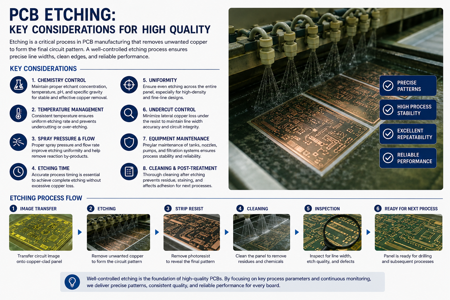

PCB Etching Process: Key Considerations for High-Quality Circuit Formation
PCB Etching Process: Key Considerations for High-Quality Circuit Formation
PCB etching is one of the most important processes in Printed Circuit Board manufacturing. It is responsible for forming the precise copper circuit patterns that enable electrical connections throughout the board.
The quality of the etching process directly affects signal integrity, impedance control, circuit accuracy, and overall PCB reliability. As modern electronic products continue to demand finer traces and higher-density designs, precise etching technology has become increasingly critical.
This article explains the PCB etching process, common challenges, and the key factors manufacturers should pay attention to in order to achieve stable, high-quality PCB production.
What Is PCB Etching?
PCB etching is the chemical process used to remove unwanted copper from the PCB surface, leaving behind the required circuit traces and pads.
The basic process includes:
- Copper-clad laminate preparation
- Dry film or photoresist application
- Circuit imaging and exposure
- Developing process
- Chemical etching
- Resist stripping
- Inspection and quality verification
After etching, the remaining copper forms the electrical pathways of the PCB.
Common PCB Etching Methods
Acidic Etching
Acidic etching solutions are widely used in PCB manufacturing because they provide:
- Better line definition
- Faster processing speed
- Stable etching performance
- Suitable results for fine-line circuits
Alkaline Etching
Alkaline etching is commonly used for inner-layer processing in multilayer PCB production.
Advantages include:
- Good copper surface quality
- Improved process consistency
- Better compatibility with photoresist systems
Different PCB designs and manufacturing requirements may require different etching chemistries.
Key Considerations in PCB Etching
1. Line Width and Spacing Control
Accurate line width and spacing are critical for modern PCB performance.
Poor etching control may cause:
- Open circuits
- Short circuits
- Signal interference
- Impedance instability
- Reduced product reliability
As PCB designs become more compact, fine-line etching capability becomes increasingly important.
2. Undercut Control
Undercut occurs when the etching solution removes copper beneath the photoresist layer.
Excessive undercut may lead to:
- Narrow trace width
- Weak conductor structures
- Reduced current capacity
- Signal performance issues
Manufacturers must optimize:
- Etching chemistry
- Spray pressure
- Temperature
- Conveyor speed
- Copper thickness
Proper process control helps achieve cleaner and more accurate circuit patterns.
3. Uniform Etching Performance
Uneven etching can create inconsistent copper thickness and circuit irregularities across the PCB panel.
To ensure uniform etching results, manufacturers should carefully monitor:
- Chemical concentration
- Solution aging
- Nozzle condition
- Spray distribution
- Equipment maintenance
Stable production conditions help improve yield and product consistency.
4. Fine-Line Capability
Advanced electronics require extremely fine traces and narrow spacing.
Applications such as:
- Smartphones
- 5G communication equipment
- Automotive electronics
- Servers and networking systems
all rely on high-precision etching technology.
Fine-line etching requires:
- High-resolution imaging
- Precise photoresist control
- Stable chemical parameters
- Advanced inspection systems
5. Copper Surface Quality
The etched copper surface directly impacts subsequent manufacturing processes such as:
- Solder mask application
- Surface finishing
- Assembly solderability
- Signal transmission
Poor surface quality may lead to:
- Oxidation
- Poor adhesion
- Increased defects
- Reliability concerns
Clean and consistent copper surfaces are essential for high-performance PCB production.
6. Environmental and Chemical Management
PCB etching involves chemical solutions that require proper environmental management.
Manufacturers should pay close attention to:
- Wastewater treatment
- Chemical recycling
- Emission control
- Worker safety
- Environmental compliance
Modern PCB factories increasingly adopt environmentally friendly manufacturing practices to improve sustainability.
Common PCB Etching Defects
Several defects may occur if the etching process is not properly controlled.
Over-Etching
Excessive copper removal can reduce trace width and weaken circuit reliability.
Under-Etching
Incomplete copper removal may cause shorts between adjacent traces.
Uneven Copper Distribution
Inconsistent etching may create impedance variation and signal instability.
Residual Copper
Unremoved copper residues can lead to electrical failures and poor isolation.
Strict quality inspection is necessary to detect and prevent these issues.
PCB Etching Inspection and Quality Control
Modern PCB manufacturers use advanced inspection systems to verify etching quality.
AOI (Automated Optical Inspection)
AOI systems inspect:
- Trace width
- Line spacing
- Shorts and opens
- Pattern defects
- Surface abnormalities
Cross-Section Analysis
Cross-sectional inspection helps evaluate:
- Copper thickness
- Sidewall profile
- Etching uniformity
- Layer structure integrity
Process Monitoring
Real-time monitoring of chemical parameters and production conditions helps maintain stable manufacturing performance.
Advanced PCB Etching Technologies
As PCB designs become more advanced, etching technologies continue to evolve.
High-Density Interconnect (HDI) Etching
HDI PCBs require ultra-fine traces and precise process control.
Modified Semi-Additive Process (mSAP)
mSAP technology supports:
- Ultra-fine circuit formation
- Reduced line width and spacing
- High-performance electronic applications
This technology is increasingly used in smartphones, wearable devices, and advanced communication products.
How High-Quality Etching Improves PCB Reliability
Reliable etching contributes to:
- Better signal integrity
- Stable impedance control
- Improved electrical performance
- Reduced defect rates
- Higher manufacturing yield
- Longer product lifespan
For industries such as automotive, aerospace, industrial automation, medical electronics, and telecommunications, precise etching quality is essential.
Conclusion
PCB etching is a highly critical manufacturing process that directly determines the accuracy and reliability of circuit formation.
By carefully controlling chemical parameters, line definition, etching uniformity, and inspection procedures, manufacturers can achieve stable and high-quality PCB production.
As electronic products continue to demand smaller sizes, faster signal transmission, and greater reliability, advanced PCB etching technology will remain a key foundation of modern electronics manufacturing.