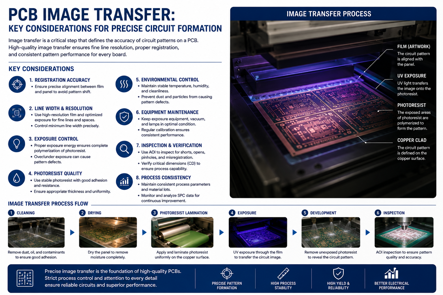

PCB Circuit Patterns: Key Considerations in the Image Transfer Process
As electronic products continue to evolve toward higher density, smaller sizes, and faster signal transmission, PCB circuit precision has become increasingly important. Even minor deviations in circuit formation may affect impedance control, signal integrity, and long-term product reliability.
This article explores the PCB image transfer process, common challenges, and the key considerations manufacturers should pay attention to in order to achieve stable and high-quality circuit production.
What Is PCB Image Transfer?
PCB image transfer is the process of transferring the designed circuit artwork onto the copper-clad laminate using photoresist materials and exposure technology.
The typical process includes:
- Surface preparation
- Dry film lamination or liquid photoresist coating
- UV exposure using artwork or direct imaging
- Developing process
- Pattern inspection
- Etching preparation
After image transfer, the exposed copper pattern becomes the foundation for the final PCB circuitry.
Importance of Accurate Circuit Formation
Accurate circuit patterns are essential for:
- Signal integrity
- Impedance control
- High-speed data transmission
- Current carrying capability
- Electrical isolation
- Product reliability
Modern PCB applications such as:
- 5G communication
- Automotive electronics
- Servers and data centers
- Medical devices
- Industrial automation
- AI hardware
all require extremely precise circuit structures.
Key Considerations in PCB Image Transfer
1. Line Width and Line Spacing Accuracy
Fine-line circuits require extremely high precision during image transfer.
Poor control may result in:
- Open circuits
- Short circuits
- Signal interference
- Impedance instability
- Reduced manufacturing yield
Manufacturers must carefully control:
- Exposure energy
- Developing parameters
- Photoresist quality
- Cleanroom conditions
2. Photoresist Quality
The photoresist layer directly affects image resolution and pattern accuracy.
High-quality photoresist helps achieve:
- Better line definition
- Improved adhesion
- Stable imaging performance
- Higher process consistency
Improper photoresist handling may lead to defects such as:
- Pattern distortion
- Poor adhesion
- Pinholes
- Incomplete development
3. Exposure Process Control
UV exposure transfers the circuit image onto the photoresist layer.
Critical factors include:
- Exposure alignment
- UV intensity
- Exposure time
- Registration accuracy
Incorrect exposure settings may cause:
- Overexposure
- Underexposure
- Inaccurate line dimensions
- Poor pattern resolution
Advanced LDI (Laser Direct Imaging) technology is increasingly used to improve imaging precision for HDI and fine-line PCB production.
4. Cleanroom Environment
PCB image transfer is highly sensitive to contamination.
Dust particles or contaminants may create defects such as:
- Open traces
- Short circuits
- Pinholes
- Pattern defects
Maintaining a controlled cleanroom environment is essential for stable production quality.
5. Registration Accuracy
Multilayer PCB production requires highly accurate layer-to-layer alignment.
Poor registration may lead to:
- Via misalignment
- Reduced annular ring
- Signal performance issues
- Reduced reliability
Modern imaging equipment uses automated alignment systems to achieve tighter tolerances.
6. Developing Process Stability
After exposure, the developing process removes either the exposed or unexposed photoresist depending on the resist type.
Improper developing may result in:
- Residual resist
- Incomplete pattern formation
- Line damage
- Reduced etching quality
Manufacturers must optimize:
- Developing chemistry
- Temperature
- Spray pressure
- Conveyor speed
Conclusion
PCB image transfer is a highly critical manufacturing process that directly determines circuit accuracy and product reliability.
By carefully controlling photoresist quality, exposure parameters, cleanroom conditions, registration accuracy, and inspection procedures, manufacturers can achieve stable and high-performance PCB production.
As modern electronics continue to demand finer circuits and higher-density designs, advanced imaging technology and strict process control will remain essential to the future of PCB manufacturing.