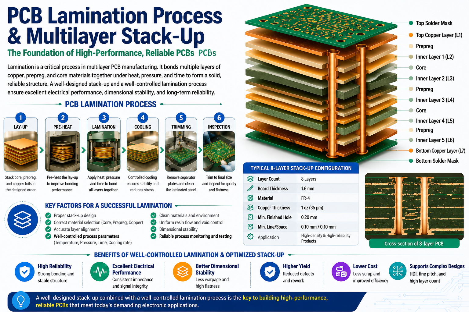

PCB Lamination & Multilayer Stack-up: The Foundation of Reliable Electronics
In PCB manufacturing, lamination and stack-up design are key processes that directly determine product reliability and electrical performance.
A well-controlled lamination process ensures strong interlayer bonding, stable structure, and consistent quality—especially for today’s high-density and high-speed applications.
📌 Key highlights of PCB lamination & stack-up:
✔ Precise layer alignment and structure design
✔ Controlled resin flow and curing during lamination
✔ Optimized material selection (FR-4, prepreg, copper foil)
✔ Stable press parameters: temperature, pressure, and time
✔ Symmetrical stack-up for reduced warpage
✔ Reliable inspection for internal quality assurance
In multilayer PCB design, stack-up configuration is critical for:
⚡ Signal integrity
⚡ Impedance control
⚡ EMI/EMC performance
⚡ Power distribution stability
⚡ Manufacturing yield and reliability
From telecommunications and automotive electronics to industrial and medical applications, high-performance PCBs all rely on precise lamination and well-engineered stack-up structures.
👉 As electronics continue to evolve toward higher speed and miniaturization, advanced lamination technology remains a core foundation of PCB manufacturing.