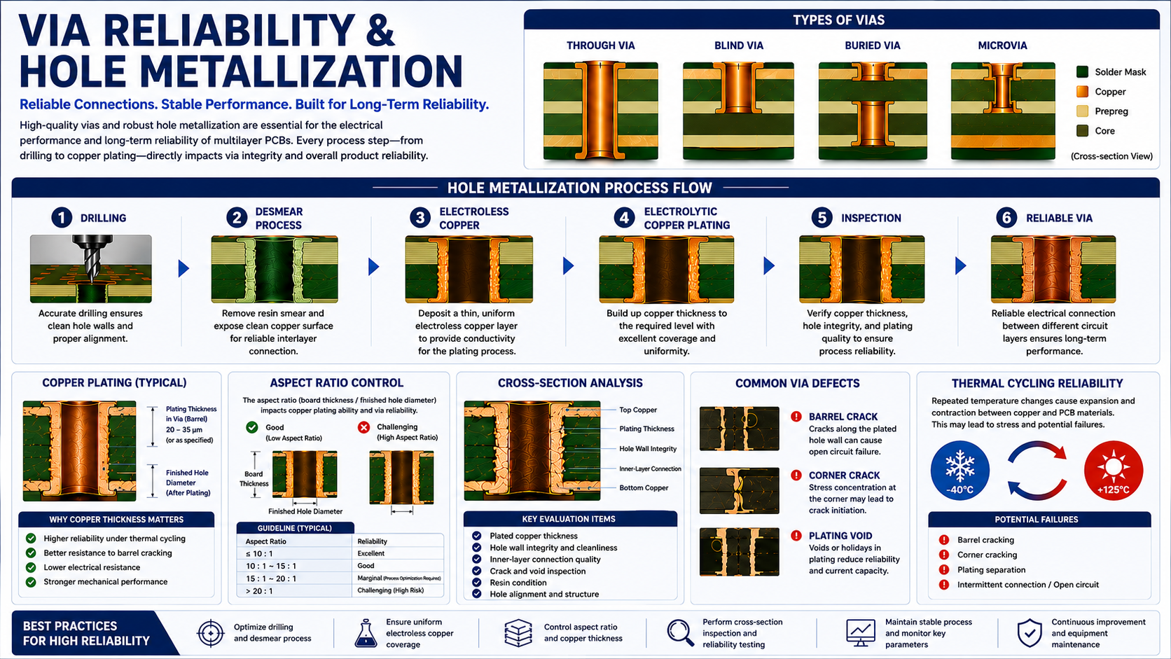

Via Reliability and Hole Metallization: Key Factors in High-Reliability PCB Manufacturing
In modern Printed Circuit Board (PCB) manufacturing, vias are essential for creating reliable electrical connections between different circuit layers. As PCB designs become more complex, with higher layer counts, smaller hole diameters, and increased thermal and mechanical demands, via reliability and hole metallization quality have become critical factors in overall PCB performance.
A reliable via must provide stable electrical conductivity and maintain mechanical integrity throughout the entire service life of the product. Any weakness in the hole wall or copper plating structure can lead to electrical failure, intermittent connections, or long-term reliability problems.
What Is a PCB Via?
A via is a plated hole that electrically connects different conductive layers within a PCB.
Common types of vias include:
Through Vias
A through via extends through the entire thickness of the PCB and can connect multiple layers.
Blind Vias
A blind via connects an outer layer to one or more internal layers without passing through the entire board.
Buried Vias
A buried via is located entirely within the internal layers of a multilayer PCB.
Microvias
Microvias are very small vias typically created by laser drilling and are widely used in HDI (High-Density Interconnect) PCB designs.
Regardless of the via type, reliable hole metallization is essential for maintaining electrical and mechanical performance.
What Is Hole Metallization?
Hole metallization is the process of depositing conductive copper onto the inner walls of drilled holes.
The basic process generally includes:
- Mechanical or laser drilling
- Hole cleaning and desmear
- Conditioning and activation
- Electroless copper deposition
- Electrolytic copper plating
- Inspection and quality verification
The final copper layer inside the hole creates a continuous electrical connection between different PCB layers.
Why Via Reliability Matters
Vias are exposed to various stresses during PCB manufacturing and product operation, including:
- Thermal cycling
- Mechanical stress
- Expansion and contraction
- Electrical current
- High-temperature processing
Differences in the coefficient of thermal expansion (CTE) between PCB materials and copper can create stress in the plated hole wall.
Over time, this stress may lead to:
- Barrel cracks
- Corner cracks
- Interlayer separation
- Plating fractures
- Intermittent electrical connections
For high-reliability applications, via integrity is therefore a critical quality requirement.
Key Factors Affecting Via Reliability
1. Drilling Quality
The quality of the drilled hole directly affects subsequent metallization.
Poor drilling conditions may result in:
- Rough hole walls
- Excessive burrs
- Resin smear
- Hole diameter variation
- Mechanical damage to inner copper layers
Proper drill bit selection, tool wear control, spindle speed, and feed rate are essential for achieving clean and consistent holes.
2. Effective Desmear Process
During drilling, heat and mechanical friction may cause resin to smear over the exposed inner copper layers.
If resin smear is not properly removed, it can prevent reliable electrical contact between the hole wall copper and the internal copper layers.
An effective desmear process helps ensure:
- Clean inner-layer copper surfaces
- Improved copper adhesion
- Reliable interlayer electrical connections
- Better plating quality
The desmear process must be carefully controlled to avoid excessive attack on the substrate or copper surfaces.
3. Electroless Copper Deposition
Electroless copper provides the initial conductive layer inside the drilled hole.
A uniform and continuous copper coating is essential before the board enters the electrolytic plating process.
Important control factors include:
- Chemical concentration
- Bath temperature
- Processing time
- Solution activity
- Surface activation
Poor electroless copper coverage may result in weak or incomplete electrical connections.
4. Electrolytic Copper Plating
Electrolytic copper plating builds the required copper thickness on the hole walls and PCB surface.
The plating process must achieve:
- Uniform copper distribution
- Adequate hole wall thickness
- Strong copper adhesion
- Good coverage at the hole entrance and center
Poor plating distribution may lead to thin areas that become vulnerable during thermal cycling.
5. Aspect Ratio Control
The aspect ratio is the relationship between PCB thickness and finished hole diameter.
As the aspect ratio increases, it becomes more difficult to achieve uniform copper plating throughout the hole.
High-aspect-ratio designs require careful consideration of:
- Hole size
- Board thickness
- Plating capability
- Chemical circulation
- Current distribution
PCB design and manufacturing capabilities must be evaluated together to ensure reliable production.
6. Copper Thickness and Distribution
The thickness of plated copper inside a via is a key factor in reliability.
Insufficient copper thickness may increase the risk of:
- Barrel cracking
- Thermal fatigue
- Electrical resistance
- Open circuits
Consistent copper distribution is particularly important for automotive, industrial, aerospace, medical, and other high-reliability applications.
Thermal Cycling and Via Reliability
One of the most important reliability tests for plated through holes is thermal cycling.
During operation, the PCB may repeatedly experience temperature changes. Copper and dielectric materials expand and contract at different rates.
Repeated thermal stress can eventually cause:
- Copper fatigue
- Barrel cracks
- Corner cracks
- Plating separation
A reliable via structure must withstand repeated thermal cycles without losing electrical continuity.
Cross-Section Analysis and Quality Inspection
Cross-section analysis is one of the most effective methods for evaluating via reliability and hole metallization quality.
A typical cross-section inspection can evaluate:
- Plated copper thickness
- Hole wall integrity
- Inner-layer connection quality
- Barrel structure
- Crack formation
- Resin condition
- Hole alignment
Cross-section analysis is especially important for:
- Multilayer PCBs
- HDI boards
- High-reliability applications
- Automotive electronics
- Aerospace products
- Medical devices
Other inspection methods may include:
- Microsection analysis
- Electrical continuity testing
- Thermal stress testing
- Plating thickness measurement
- Automated optical inspection
Common Via and Hole Metallization Defects
Typical defects may include:
Barrel Cracks
Cracks along the plated copper barrel can interrupt electrical continuity.
Corner Cracks
Stress concentration near the transition between the hole wall and internal copper layers may lead to cracking.
Voids in Plating
Missing copper areas can create weak points in the electrical connection.
Poor Inner-Layer Connection
Insufficient cleaning or poor metallization may prevent reliable contact with internal copper layers.
Uneven Copper Plating
Non-uniform plating thickness can reduce long-term reliability.
Early detection and effective process control are essential to prevent these defects.
How to Improve Via Reliability
To achieve stable and reliable via performance, PCB manufacturers should focus on:
- Optimized drilling parameters
- Effective desmear treatment
- Stable electroless copper deposition
- Uniform electrolytic copper plating
- Proper aspect ratio design
- Consistent copper thickness
- Strict chemical process control
- Regular equipment maintenance
- Cross-section inspection
- Thermal reliability testing
A combination of process control, engineering capability, and quality inspection is essential for achieving long-term via reliability.
Conclusion
Via reliability and hole metallization are fundamental to the performance of modern multilayer PCBs.
From drilling and desmear to electroless copper and electrolytic plating, every process step contributes to the final quality of the plated hole.
As electronic products continue to demand higher density, smaller vias, higher speeds, and greater reliability, advanced hole metallization technology and strict process control will remain essential in PCB manufacturing.
A reliable PCB starts with reliable interlayer connections.
By maintaining precise drilling, stable copper plating, accurate process control, and comprehensive inspection, manufacturers can produce PCBs capable of meeting the demanding requirements of modern electronic applications.